 English
 Vietnamese
 Italian
 Spanish
 Thai
Thai Japanese
 Portuguese
 Korean
 Russian
 French
 German
 Polish
 Indonesian
How to Select the Right SMD Inductor for High-Density PCB Designs
High-density PCBA designs place strict demands on power circuits. An incorrect SMD inductor can cause thermal issues and EMI noise in the PCB layout. Overheating, magnetic saturation, and signal interference often result from limited board space. Successful smd inductor selection requires careful balance of size, electrical performance, and thermal management. Engineers must evaluate key specifications, such as saturation current and self-resonant frequency. They also need to consider the application's specific requirements. Proper surface-mount technology choices enhance reliability in dense layouts. The designer must understand how to choose an smd inductor that meets both current and space constraints. This selection process directly impacts the design's overall performance and longevity. Inductor performance under high current conditions is critical.
How to Choose an SMD Inductor: Key Specifications
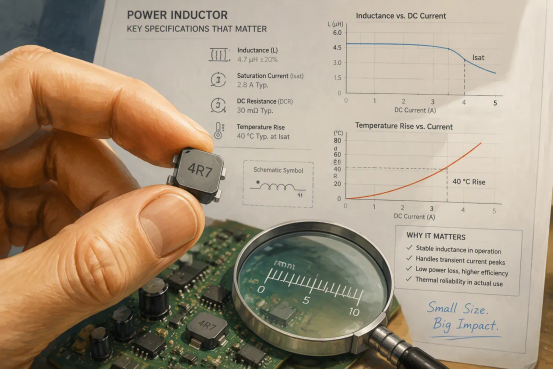
Selecting the right component begins with understanding the key smd inductor specifications that govern performance in dense layouts. Engineers must evaluate several electrical parameters before committing to a part number. These parameters determine whether the inductor will operate reliably under real-world conditions or fail prematurely. The most critical specifications include inductance value, rated current, saturation current, DCR, Q factor, and self-resonant frequency. Each parameter interacts with the others, and the selection process requires balancing them against the application's demands.
Saturation Current and Rated Current
Saturation current (Isat) represents the current level at which the inductance drops by a specified percentage, typically 20-30% from its zero-current value. For SMD Tiny Power Chokes, this drop is commonly defined at -35% inductance relative to the initial measurement. When the core saturates, the inductor loses its magnetic effectiveness, and the circuit experiences instability. The current surges like a short circuit, potentially destroying the switching transistor or triggering overcurrent protection. This failure mode becomes especially dangerous in high-density designs where thermal and space margins are tight.
Rated current (Irms) defines the maximum DC current the inductor can carry without exceeding a specified temperature rise. For a double choke, each winding passing its rated current causes a +20°C rise, and both windings together sum to +40°C, which represents the conservative thermal limit. These two ratings are independent constraints. The saturation current must exceed the peak inductor current, calculated as the average input current plus half the ripple current. Engineers should select an smd inductor with Isat at least 20-25% higher than the peak to provide margin for thermal variation and aging. Meanwhile, the rated current must handle the continuous thermal load without excessive I²R losses.
According to the LCSC guide, saturation current ratings for SMD inductors typically span from 10 mA to 30 A. For power inductors used in DC-DC converters, ratings up to 30 A are common. High-current flat-wire power inductors push these limits further. The IN Series reaches a maximum saturation current of 85 A, while the LP05 Series achieves 55 A. The LP06 Series delivers 75 A, the LP07 Series reaches 85 A, and the LP08 Series provides 45 A. These components demonstrate that high-density PCB designs can accommodate substantial current demands when the correct part is chosen.
Self-Resonant Frequency and DCR
Self-resonant frequency (SRF) marks the point where the inductor's parasitic capacitance resonates with its inductance. Above this frequency, the component behaves capacitively rather than inductively. The operating frequency must remain well below the SRF to maintain proper inductive behavior. High-density designs often push switching frequencies higher to shrink passive component sizes, making SRF a critical check during smd inductor selection.
DC resistance (DCR) directly causes I²R power loss in the winding. Lower DCR values reduce conduction losses and improve overall efficiency, especially in high-current paths. The Q factor measures the inductor's efficiency at a specific frequency, representing the ratio of reactance to resistance. Different applications demand different Q-factor targets. High-frequency resonance circuits and RF filters require very high Q to minimize energy loss and maintain signal integrity. Power-side coupling and energy transfer applications need low to medium Q with very low DCR to minimize conduction losses. Power filter chokes and SMPS DC-DC inductors both prioritize very low DCR as the primary factor for efficiency, since resistive losses directly impact power conversion performance.
Core material also influences efficiency. Ferrite and nanocrystalline cores exhibit low core loss at high frequencies, reducing energy waste during high-speed switching. Iron powder cores cost less but perform poorly at high frequencies. The trade-off between low loss and cost directly affects the efficiency target versus budget in high-density designs. Thermal management remains equally important, as poor heat dissipation degrades efficiency and reliability in enclosed, space-constrained PCBs.
SMD Inductor Selection: Balancing Size and Thermal Performance
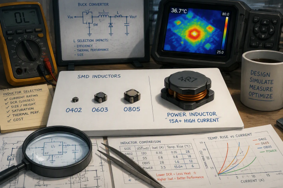
The physical footprint of an smd inductor directly influences its electrical capabilities. Designers face a fundamental tension: smaller packages conserve precious board area, but they also constrain the winding geometry and core volume. These constraints raise DCR and lower saturation current. The result is a component that generates more heat while carrying less current. Engineers must evaluate this trade-off carefully during smd inductor selection.
Choosing the Right Package for Current Needs
Standard package sizes such as 0402, 0603, and 0805 represent common starting points for many designs. Each size offers distinct advantages and limitations. A 0402 package occupies minimal space, making it attractive for ultra-compact layouts. However, its tiny winding area forces higher resistance and reduces the conductor cross-section. The saturation current drops accordingly, limiting the component to low-power applications. A 0603 package provides a middle ground, balancing footprint against moderate current capability. The 0805 package handles higher currents more comfortably, but its larger footprint consumes valuable board space.
The selection process must match the package to the actual current demand. For example, a DC-DC converter delivering 2 A continuous current requires an inductor with a saturation current well above that level. A small 0402 package typically cannot meet this requirement without saturating. The designer must move to a larger package or select a specialized high-current construction. High-current flat-wire power inductors demonstrate this principle clearly. The IN Series reaches a maximum saturation current of 85 A, while the LP05 Series achieves 55 A. These components use larger footprints and optimized windings to deliver substantial current handling. The LP06 Series delivers 75 A, the LP07 Series reaches 85 A, and the LP08 Series provides 45 A. These options show that high-density designs can accommodate significant current demands when the correct part is chosen.
Managing Heat Dissipation with Low DCR
DC resistance determines the resistive power loss in the winding. The power dissipated equals the square of the current multiplied by the resistance. A lower DCR value directly reduces this loss, keeping the component cooler during operation. This relationship becomes critical in dense boards where airflow is restricted and adjacent components radiate heat. Thermal management is essential in high-density designs, and selecting an inductor with good thermal performance is a primary consideration.
Copper thickness plays a significant role in DCR performance. Adequate copper cross-section lowers resistance and improves heat spreading across the component body. Thicker windings also conduct heat away from the core more effectively. The rated current specification reflects this thermal behavior. For a double choke, each winding passing its rated current causes a +20°C rise, and both windings together sum to +40°C, representing the conservative thermal limit. Engineers should verify that the continuous operating current stays below this rated value to prevent excessive temperature rise.
The application's efficiency target also influences the DCR requirement. Power filter chokes and SMPS DC-DC inductors both prioritize very low DCR as the primary factor for efficiency. Resistive losses directly impact power conversion performance, so minimizing DCR improves overall system efficiency. Core material selection also affects thermal behavior. Ferrite and nanocrystalline cores exhibit low core loss at high frequencies, reducing energy waste during high-speed switching. Iron powder cores cost less but perform poorly at high frequencies, generating more heat. The trade-off between low loss and cost directly affects the efficiency target versus budget in high-density designs. A well-chosen smd inductor balances package size, DCR, and current capability to meet both thermal and electrical requirements.
Shielded vs. Unshielded Inductors for EMI Control
Electromagnetic interference poses a serious challenge in high-density PCB layouts. The magnetic field generated by an inductor can radiate into surrounding circuitry, causing crosstalk and signal degradation. This problem intensifies as board space shrinks and component density increases. The choice between shielded and unshielded constructions directly affects EMI performance and overall design success.
Attribute | Unshielded SMD Inductor | Shielded SMD Inductor |
Magnetic field containment | Radiates freely into surrounding space | Confined within the component using magnetic/composite structure |
EMI risk | Higher risk, especially in compact or noise-sensitive designs | Significantly reduced radiated noise |
Interaction with nearby components | Higher interaction with traces and components | Minimized interaction, beneficial for high-density PCB layouts |
Cost/Efficiency | Often lower cost, sometimes higher efficiency due to reduced core losses | Not specified in this evidence segment |
When to Choose Shielded Inductors
Shielded inductors use a magnetic or composite structure that confines the magnetic field within the component body. This construction prevents stray flux from leaking into adjacent traces, vias, and sensitive analog circuits. Designers should prefer shielded types when the inductor sits near high-impedance nodes, precision measurement circuits, or RF front-ends. High-frequency switching converters also benefit from shielding because the rapid current transitions generate strong magnetic pulses that easily couple into nearby conductors.
The advantages extend beyond immediate circuit performance. Reduced stray magnetic fields help maintain signal integrity across the entire board. This improvement simplifies compliance with EMC standards during certification testing. Engineers often save considerable time during troubleshooting because shielded components eliminate a common noise source. For high-density designs where multiple power rails operate in close proximity, the isolation provided by shielded inductors proves essential. The smd inductor selection process should prioritize shielding whenever layout constraints force sensitive circuitry near power paths.
Impact on Footprint and Cost
Shielded constructions typically require additional material around the winding to contain the magnetic flux. This extra structure increases the component height and footprint compared to unshielded equivalents. The added manufacturing complexity also raises the unit cost. Designers must weigh these penalties against the EMI benefits. Unshielded inductors offer a smaller profile and lower price, making them attractive for cost-sensitive consumer products with generous board space.
However, the cost calculation changes when EMI countermeasures become necessary. Adding ferrite beads, shielding cans, or additional filtering components to compensate for an unshielded inductor often costs more than selecting a shielded part initially. The total system cost, not just the component price, should guide the decision. For automotive, medical, and industrial applications where reliability and certification matter, shielded inductors represent the safer choice. The how to choose an smd inductor process must account for these system-level trade-offs. A shielded inductor that prevents a redesign cycle delivers better value than a cheaper part that creates compliance problems.
Selecting the Right SMD Inductor Construction
The internal construction of an smd inductor determines its performance envelope more than any other factor. Engineers must understand how each manufacturing approach shapes electrical behavior, thermal characteristics, and physical dimensions. The smd inductor selection process narrows significantly once the construction type matches the application's frequency and current demands.
Wirewound and Multilayer Inductors
Wirewound inductors use a coil of insulated copper wire wrapped around a ferrite or iron core. This construction delivers high current handling and low DCR because the wire cross-section remains substantial. Vertical winding techniques allow the coil to stand upright, reducing the footprint while maintaining inductance. This orientation proves valuable in high-density pcb layouts where horizontal space is scarce. Wirewound parts excel in power conversion circuits that demand stable inductance under heavy loads.
Multilayer inductors stack thin ceramic or ferrite layers with printed conductive patterns. The manufacturing process creates a compact, monolithic component with excellent high-frequency behavior. These parts suit RF filtering and signal conditioning where parasitic capacitance must stay minimal. However, multilayer construction limits current capacity compared to wirewound equivalents. The thin conductive traces increase resistance, generating more heat under sustained load. Designers choose multilayer parts when board space outweighs current requirements.
Molded and Thin-Film Inductors
Molded inductors use a compression-molding process that embeds the winding in a magnetic compound. This technique reduces flux leakage and improves saturation-current behavior. The molded structure delivers higher power density and stronger EMI suppression than conventional wound inductors. These components suit high-power DC-DC converters and CPU/GPU power rails where board space is at a premium.
The advantages of molded construction include:
· Ultra-low buzzing noise from the molded structure, improving data center user experience
· Extremely low core loss with excellent soft saturation for high-frequency operation
· Slim design that saves installation space for high-density mounting
· Wide operating temperature range from -55°C to +170°C for harsh environments
· AEC-Q200 qualification ensuring high reliability for automotive systems
For AI processor applications, molded inductors offer inductance ranges of 56–82 nH with DCR as low as 0.19 mΩ. These ultra-low-voltage, high-current rails sit closest to processor dies. The compact footprint enables miniaturization while extended temperature ranges support sustained thermal loading. Automotive systems benefit from robust construction against vibration and shock, critical for on-board chargers, battery management systems, and advanced driver assistance systems.
Thin-film inductors use precision deposition techniques to create extremely accurate, low-profile components. They excel in RF applications requiring tight tolerance and stable temperature coefficients. The manufacturing process limits current capacity, making them unsuitable for power delivery. The how to choose an smd inductor decision ultimately depends on whether the circuit prioritizes power handling or signal precision. Each construction type serves a distinct purpose, and the selection must reflect the design's primary objective.
Successful smd inductor selection begins with defining critical specifications. Engineers must verify saturation current exceeds peak current, confirm SRF sits above operating frequency, and check DCR against thermal budgets. The size-thermal trade-off demands careful package evaluation. Shielding decisions depend on EMI requirements and nearby sensitive circuits. Construction type must match the application's frequency and current needs.
No single best inductor exists. The right choice depends entirely on specific design constraints. Each pcb layout presents unique challenges requiring different solutions.
Final Checklist: Before finalizing, verify saturation current exceeds peak current, SRF remains above operating frequency, DCR meets thermal budget, and package fits layout with adequate heat dissipation clearance. This inductor selection workflow ensures reliable performance in dense designs.
FAQ
What happens if an inductor saturates during operation?
Saturation causes the inductance to drop sharply, often by 20-30% from its rated value. The component then behaves like a short circuit, allowing excessive current to flow. This condition can damage switching transistors or trigger protection circuits. Engineers must verify the saturation current exceeds the peak operating current with adequate margin.
How does package size affect thermal performance?
Smaller packages like 0402 offer limited winding space, which increases DCR and reduces current capability. Higher DCR generates more heat through I²R losses. A larger package allows thicker copper windings, lowering resistance and improving heat dissipation. The selection process must balance footprint constraints against thermal requirements.
When should a designer choose a shielded inductor?
Shielded inductors confine the magnetic field within the component body, reducing EMI and crosstalk. Designers should select shielded types when the inductor sits near sensitive analog circuits, high-frequency switching nodes, or RF front-ends. The added material increases footprint and cost, but prevents expensive redesign cycles caused by interference problems.
What is the difference between rated current and saturation current?
Rated current defines the maximum DC current without exceeding a specified temperature rise, typically +20°C to +40°C. Saturation current marks the point where inductance drops by a specified percentage. Both constraints matter during smd inductor selection. The rated current handles continuous thermal load, while saturation current must cover peak transient conditions.
How does the inductor selection workflow begin?
The workflow starts with defining key smd inductor specifications: inductance value, saturation current, DCR, and self-resonant frequency. Engineers then evaluate package size against current demands and thermal budgets. Shielding decisions follow based on EMI requirements. Finally, construction type matches the application's frequency and power needs. This systematic approach ensures reliable performance in dense pcb layouts.