English
 Vietnamese
 Italian
 Spanish
 Thai
 Japanese
 Portuguese
 Korean
 Russian
 French
 German
 Polish
 Indonesian
SMD Inductor Footprint Design and Solder Joint Reliability in PCB Assembly
Footprint design governs solder joint reliability. Copper geometry sets solder volume, fillet shape, and stress distribution.
Design engineers and assembly specialists can control several parameters: pad size, pad shape, pad spacing, thermal relief, component orientation, and the choice between NSMD and SMD pads. Each choice prevents a specific failure mode: tombstoning, joint cracking, or thermal fatigue.
An SMD inductor depends entirely on its solder joints. Those joints carry mechanical load, electrical current, and heat. A weak joint compromises all three functions at once. Inductor footprints deserve the same scrutiny as the part itself.
This guide offers practical rules for footprint decisions. Readers can apply them during layout and verify them at assembly.
Key Parameters in SMD Inductor Footprint Design
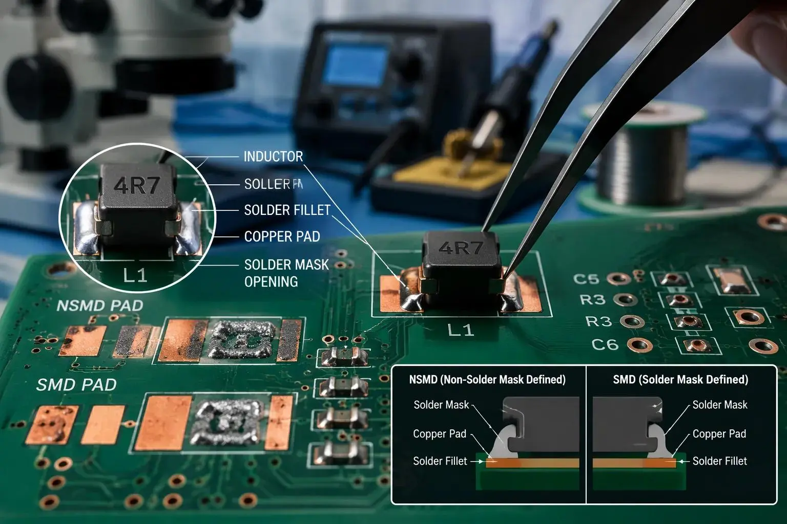
A properly designed footprint ensures reliable solder joints, accurate placement, manufacturability, and electrical and thermal performance. An inaccurate footprint causes poor joints, misalignment, or unassemblable boards even when the schematic and routing are correct. JLCPCB notes that incorrect footprints produce weak joints, excess solder shorts, tombstoning, skewing, and long-term reliability loss from cracked joints. SLLPCB adds misaligned leads, open joints, solder bridges, and assembly rejection to that list. Good smd inductor footprint design therefore starts with three levers: pad dimensions, pad shape and spacing, and mask definition.
Pad Dimensions and Solder Volume
Copper pads typically measure about 80% of the ball or pad size, a ratio that sets proper solder volume. A typical toe extension of 0.2–0.5 mm and heel of 0.1–0.3 mm, which industry standards associate with roughly 15% joint reliability improvement, give the fillet room to form. Pads that are too small, too large, or incorrectly positioned lead to poor solder joints, according to SLLPCB. Pad size and spacing also govern paste release. JLCPCB recommends a 5–10% aperture reduction to prevent excess solder deposition, component float, bridging, and thermal imbalance. The recommended land pattern for each inductor comes from the manufacturer's datasheet, and IPC-7351 land pattern density levels help designers choose between density grades. These pad spacing and dimensions rules apply to every land pattern, from tiny chip parts to large shielded parts.
NSMD vs. SMD Pads and 0603 SMD Package Footprints
NSMD (non-solder-mask-defined) pads improve solder joint reliability versus SMD pads, because the mask opening exceeds the copper and the fillet wraps the pad sides. SMD pads suit dense routing where mask anchoring helps. Both fit different design contexts. The 0603 SMD package footprints show the tradeoff at small scale. These 0603 package footprints demand tight pad proportions and spacing, and JLCPCB ties paste release consistency directly to package size. The 0603 package footprints also sit in the 100–120 µm stencil thickness band, so aperture design matters as much as copper geometry. Designers who treat 0603 package footprints as miniature versions of larger parts often lose yield. The 0603 package footprints reward exact CAD footprint design.
Package Size | Ideal Stencil Thickness |
01005 / 0201 | 80–100 µm |
0402 / 0603 | 100–120 µm |
0805+ | 120–150 µm |
SMD inductor footprints typically consist of two pads, and designers can combine them with a solder ball to manage circuit connections. Pad shape and spacing decide how that joint wets. A balanced copper footprint pads pair keeps surface tension symmetric. These smd inductor footprints and layouts decisions feed directly into solder joint reliability, so teams should document them in their inductor PCB layout best practices. Surface mount inductor footprint design and footprint design and placement belong together in one review. Inductor packages and footprints vary widely, and each inductor needs its own verified footprint. PCB design teams should treat every footprint as a controlled artifact, not a copy-paste leftover.
Failure Modes and Solder Joint Reliability
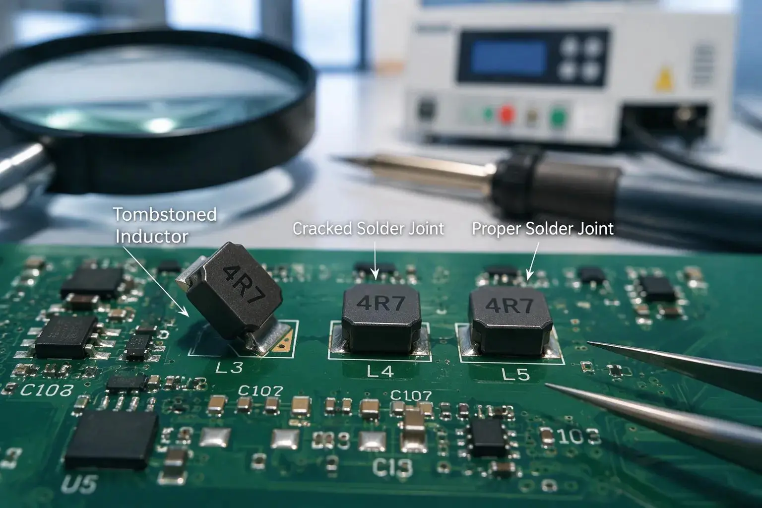
Two failure modes dominate field returns on SMD inductors: tombstoning during reflow and joint cracking over service life. Each one traces back to specific footprint parameters. Pad imbalance, spacing, mask definition, and orientation all shape how a joint forms and how it survives stress.
Tombstoning and Uneven Wetting
Tombstoning occurs when a two-terminal SMD component is pulled upward on one side during reflow soldering. The cause is an imbalance between the two component ends, as Beeproduced explains. The critical moment arrives when the solder paste on both pads melts, wets the termination surfaces, and spreads between pad and termination. Ideally, both pads heat evenly, the paste liquefies almost simultaneously, and the resulting forces balance out. Trouble starts when wetting begins earlier or more strongly on one side. The liquid solder on that side pulls on the component while no equal counterforce exists on the opposite side. Small, lightweight parts lift easily under that imbalance.
Several triggers create the wetting-force imbalance, according to JLCPCB:
Trigger of wetting-force imbalance | Detail |
Heating ramp too fast | One pad reaches the alloy's liquidus temperature before the other |
Uneven copper heat distribution | One pad connects to a massive ground plane while the other stays isolated |
Paste volume mismatch | Mismatch between the two pads |
Asymmetric pad heating | Within the oven's convection zones |
PCBCart adds pad design problems to the list: pads of different size, separation, or copper connection produce unequal solder volumes or heating behavior. Off-center placement lets solder on one side grab the termination and drag the device upward. Flux activity, paste viscosity, surface finish, contamination, and oxidation also shift wetting speed. Tombstoning prevention therefore starts in layout. Symmetric pads, balanced copper connections, and centered placement remove the root cause. A controlled reflow profile with a slow start, a constant soak area, and a correct peak temperature lets both joints melt concurrently.
Cracking and Thermal Fatigue
Cracked joints occur when thermal or mechanical stress breaks the solder connection through poor pad stress distribution, according to PCBMaster. Thermal cycling expansion mismatch drives the process. A stiff joint geometry concentrates stress at the heel, and repeated cycles propagate a crack until the joint opens. Weak pad design raises stress concentration, and the problem appears most often in automotive and industrial environments. Incorrect pad size or asymmetry, poor solder mask and paste mask alignment, and insufficient thermal balance between pads all contribute. Ignoring IPC design standards compounds the risk.
Mitigation options depend on context. PCBMaster recommends IPC-7351 pad libraries, symmetrical pad pairs for SMT components, optimized paste aperture design, improved thermal balance for small components, and proper solder mask spacing to avoid bridging. DFM checks before fabrication catch footprint mismatch errors early. Designers working with 0603 package footprints should note that small bodies tolerate less asymmetry than larger parts, so the same imbalance that merely skews a big inductor will tombstone a 0603 part. These 0603 package footprints also leave less copper for heat spreading, which raises local thermal stress. A footprint review that pairs balanced geometry with a validated reflow window protects solder joint reliability across both failure modes.
Thermal and Mechanical Considerations
CTE Mismatch and Thermal Relief
An inductor and its PCB expand at different rates during thermal cycling. The board, the copper, and the component body each carry a different coefficient of thermal expansion. This mismatch strains the solder joint with every temperature swing. A stiff joint concentrates that strain at the heel, where the fillet meets the pad. Repeated cycles then propagate a crack until the connection opens.
Thermal relief shapes how heat moves through the joint. A pad tied directly to a large copper plane conducts heat away quickly during reflow. That fast sink can leave one termination cooler than the other and delay wetting on that side. Thermal relief spokes slow the heat path and balance the two ends. Designers should weigh this benefit against current-carrying needs, because narrow spokes add resistance. The right balance depends on the inductor's power level and the surrounding copper area.
Orientation and Stress Distribution
Component orientation changes the stress path through the joint. An inductor placed parallel to a board edge sees bending stress along its long axis. Rotation by ninety degrees shifts that load onto the weaker direction. Layout reviews should check orientation against known board flex points, mounting holes, and connector areas.
Pad symmetry supports even stress distribution. Asymmetric pads load one fillet harder than its partner. Symmetric geometry, verified against IPC-7351 land patterns, spreads the load across both joints. Good footprint design pairs that symmetry with a sensible orientation. Teams should record both choices in their footprints library, so later projects inherit a proven layout. This discipline protects solder joint reliability across the product life.
SMD Inductor Footprint Guidelines for Assembly
Footprint choices flow directly into stencil aperture design and the reflow profile window. A pad that is too large demands a reduced aperture; a pad tied to heavy copper needs a slower soak. These smd inductor footprint guidelines tie layout decisions to the assembly line.
SMT assembly can achieve 5.5 to 20 solder joints per square centimeter with high impact and vibration resistance. Footprint design supports that density. Balanced pads hold paste volume steady, and steady volume keeps every joint in the window. Teams without in-house process control can rely on professional PCB assembly services for SMD shielded inductors. That route suits low-volume teams; it is one option, not a requirement.
Stencil Design and Reflow Profile
Aperture size follows pad geometry. Designers reduce the aperture by 5–10% against the copper to prevent excess paste, component float, and bridging. The 0603 package footprints sit in the 100–120 µm stencil band, so aperture precision matters more there than on larger parts. Reflow soldering succeeds when both terminations reach liquidus together. A slow ramp and a constant soak balance the two ends. The same logic appears in inductor pcb layout best practices: symmetric copper, symmetric heat.
Inspection and Process Control
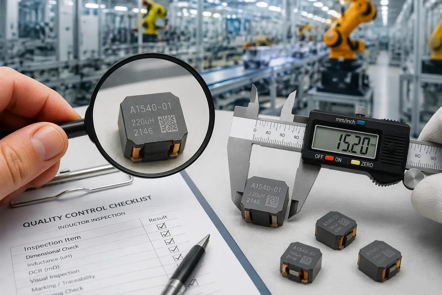
Inspection closes the loop. Visual checks catch tombstoning and skew. X-ray reveals voids and hidden fillets under shielded bodies. Cross-section confirms fillet shape on critical parts. Each result feeds back into footprint revision. A recurring void points to an aperture change; a cracked heel points to pad geometry. This feedback turns surface mount inductor footprint design into an iterative discipline. Good manufacturing and assembly considerations include that loop from day one.
Footprint Best-Practices Checklist
The table below condenses the parameters covered in earlier sections into a single review sheet. Each row points back to the section that explains the reasoning.
Parameter | Target | Section |
Pad ratio | Copper pads near 80% of the pad or ball size | Pad Dimensions and Solder Volume |
Toe extension | 0.2–0.5 mm | Pad Dimensions and Solder Volume |
Heel extension | 0.1–0.3 mm | Pad Dimensions and Solder Volume |
Mask definition | NSMD for joint reliability, SMD for dense routing | NSMD vs. SMD Pads |
Pad symmetry | Equal area and equal copper connection on both pads | Tombstoning and Uneven Wetting |
Thermal relief | Spokes sized to the inductor's power level | CTE Mismatch and Thermal Relief |
Orientation | Checked against board flex points and mounting holes | Orientation and Stress Distribution |
Stencil aperture | 5–10% reduction against copper | Stencil Design and Reflow Profile |
Stencil thickness | 100–120 µm for 0603 package footprints | NSMD vs. SMD Pads |
Reflow | Slow ramp, constant soak, matched liquidus timing | Stencil Design and Reflow Profile |
Designers should run this list during layout review, not after fabrication. A pad ratio outside the 80% target or an asymmetric pair will surface as a defect at assembly. Industry standards tie the toe and heel extensions above to roughly 15% joint reliability improvement, so the numbers carry real weight.
Two habits keep the checklist useful. First, verify every smd inductor footprints entry against the manufacturer datasheet and IPC-7351 density levels. Second, log each deviation and its inspection result. These smd inductor footprint guidelines only protect yield when teams apply them consistently across projects. Sound footprint design and disciplined inductor pcb layout best practices share the same foundation: balanced copper, verified geometry, and a documented review. Teams that treat surface mount inductor footprint design as a controlled process build a library of proven footprints. That library then shortens every future layout and keeps joint reliability predictable.
Footprint design gives engineers the first and most controllable lever for solder joint reliability. Copper geometry sets solder volume, fillet shape, and stress path before any part reaches the line.
Designers should apply the checklist parameters early in layout. They then validate each choice through assembly and inspection data. This sequence catches imbalance before it becomes a defect.
Field returns and process feedback should drive the next revision. A cracked heel or a recurring void tells teams where the footprint needs work. Each update strengthens the library. Every inductor then inherits a proven land pattern, and every new footprints review starts from evidence rather than guesswork.